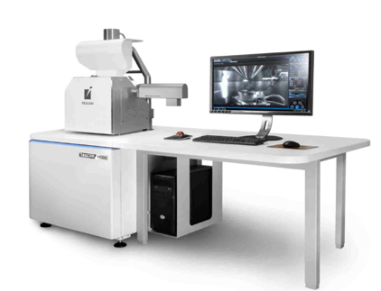
The scanning electron microscope takes its name from the method of obtaining an image using the stepping motion of the electron beam across the surface of the specimen. As the beam does not penetrate the object under examination, operating voltages from 1-30 kV are used. The primary electron beam is emitted by a cathode. Electromagnetic lenses focus the beam and coils deflect the beam, giving it a stepped motion. By deflecting the electron beam, we can regulate the magnification achieved. Electrons incident on a surface are partly scattered (BSE electrons), partly penetrate the object causing emission of secondary electrons (SE), visible light and X-rays. Detectors convert the electron signal into a digital signal, which is then converted into an image. A high vacuum is maintained in the microscope column.
The resolution capacity of the scanning microscope is dependent on the beam diameter and does not exceed several hundred thousand times.